
|
39.832 bytes |
Product Information |
Document ID: MCGN-45WU9P |
Netfinity 5500 M20 - Processor board component locations and processor board jumpers
Applicable to: World-Wide
Source: Hardware Maintenance Manual
Processor board component locations
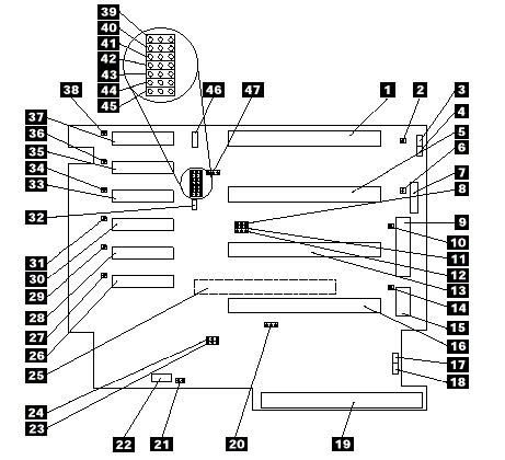
A layout of the processor board is shown in the following illustration.

1 Microprocessor 1 connector (J1)
2 Microprocessor 1 error LED (CR16)
3 Microprocessor 1 fan power connector (J7)
4 Microprocessor 2 fan power connector (J8)
5 Microprocessor 2 connector (J2)
6 Microprocessor 2 error LED (CR15)
7 Power control connector (to power backplane) (J33)
8 Reserved (might not be present) (J15)
9 Power connector (to power backplane) (J32)
10 Microprocessor 3 error LED (CR18)
11 Reserved (might not be present) (J22)
12 Reserved (might not be present) (J23)
13 Microprocessor 3 connector (J3)
14 Microprocessor 4 error LED (CR21)
15 Power connector (J35)
16 Microprocessor 4 connector (J4)
17 Microprocessor 3 fan power connector (J9)
18 Microprocessor 4 fan power connector (J10)
19 Memory board connector
20 Reserved (J24)
21 Reserved (J37)
22 Fan 4 connector (J36)
23 Reserved (might not be present) (J21)
24 Reserved (J20)
25 System board connector (on reverse side of processor board)
26 VRM 6 connector (J18)
27 VRM 6 error LED (CR4)
28 VRM 5 connector (J17)
29 VRM 5 error LED (CR7)
30 VRM 4 connector (J16)
31 VRM 4 error LED (CR2)
32 Reserved (J11)
33 VRM 3 connector (J14)
34 VRM 3 error LED (CR3)
35 VRM 2 connector (J13)
36 VRM 2 error LED (CR6)
37 VRM 1 connector (J12)
38 VRM 1 error LED (CR5)
39 - 42 Microprocessor core-frequency-selection jumper block (J31 - J28)
43 Reserved (J27)
44 Reserved (J25)
45 Reserved (J26)
46 Reserved (J19)
47 Reset system jumper block (J34)
Processor board jumpers
Table 14 contains the names and descriptions of the jumper blocks located on the processor board. Table 15 shows the microprocessor core-frequency-selection jumper settings. The highlighted numbers in the table refer to the highlighted numbers in the illustration in "Processor board component locations".
|
Notes |
|
Attention |
Table 14. Processor board jumpers
|
Jumper Name |
Description |
|
20 J24 Reserved |
The default position is a jumper on pins 1 and 2. |
|
22 J37 Reserved |
The default position is a jumper on pins 1 and 2. |
|
23 J21 Reserved |
The default position is a jumper on pins 2 and 3. |
|
24 J20 Reserved |
The default position is a jumper on pins 1 and 2. |
|
39 - 42 J31 - J28 |
For the core/bus fraction 4 (400/100 MHz), jumpers are installed on pins 1 and 2 of J28, J30, and J31 and on pins 2 and 3 of J29. |
|
43 J27 Reserved |
The default position is a jumper on pins 1 and 2. |
|
44 J25 Reserved |
Reserved The default position is a jumper on pins 1 and 2. |
|
45 J26 Reserved |
The default position is a jumper on pins 2 and 3. |
|
47 J34 Reset system |
The default position for normal operation is no jumper on J34. |
|
Core/bus |
J28 |
J29 |
J30 |
J31 |
|
4 |
Pins 1 |
Pins 2 |
Pins 1 |
Pins 1 |
|
4.5 |
Pins 1 |
Pins 2 |
Pins 2 |
Pins 1 |
|
5 |
Pins 2 |
Pins 2 |
Pins 1 |
Pins 1 |
|
Search Keywords |
| |
|
Document Category |
Diagrams | |
|
Date Created |
12-03-99 | |
|
Last Updated |
21-05-99 | |
|
Revision Date |
26-03-2000 | |
|
Brand |
IBM PC Server | |
|
Product Family |
Netfinity 5500 M20 | |
|
Machine Type |
8662 | |
|
Model |
ALL | |
|
TypeModel |
| |
|
Retain Tip (if applicable) |
| |
|
Reverse Doclinks |