
|
98.377 bytes |
Service Hints & Tips |
Document ID: GSMH-3GGK4W |
Aptiva - 2161 System board layout & locations
Applicable to: World-Wide
System Board Layout
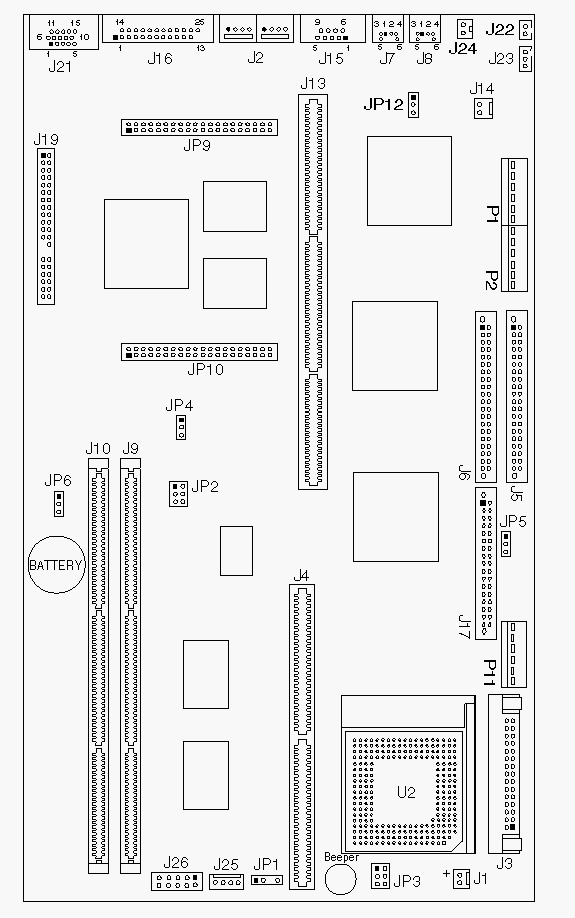
Figure 5-1. System Board
System Board Locations
|
J1 |
Fan +12 V dc connector |
|
J2 |
USB (Universal Serial Bus) |
|
J3 |
System board voltage regulator connector |
|
J4 |
Cache connector |
|
J5 |
Primary Hard Disk IDE (Hard Disk 1, Hard Disk 2) |
|
J6 |
Secondary Hard Disk IDE (Hard Disk 3 or CD-ROM, Hard Disk 4) |
|
J7 |
Mouse connector |
|
J8 |
Keyboard connector |
|
J9 |
DIMM 168-pin Socket |
|
J10 |
DIMM 168-pin Socket |
|
J13 |
Riser Connector - PCI/ISA |
|
J14 |
External speaker power connector |
|
J15 |
Serial Port connector |
|
J16 |
Parallel Port connector |
|
J17 |
Diskette drive connector |
|
J19 |
VESA feature connector (16 bit video input) |
|
J21 |
Monitor signal connector |
|
J22 |
Power Supply 2-pin connector (On/off switch) |
|
J23 |
Power Supply 3-pin connector (5 V dc) |
|
J24 |
Wake Up On Ring connector |
|
J25 |
HDD/Power-on LED connector (HDD: 1-2, Power-on: 3-4) |
|
J26 |
Media console connector - not used |
|
J27 |
Internal VGA connector |
|
JP1 |
External speaker (Internal: 1-2, External: 2-4) |
|
JP2 |
System board bus clock |
|
JP3 |
Core bus frequency ratio |
|
JP4 |
System board flash jumper (Normal: 1-2, Write protect: 2-3) |
|
JP5 |
Diskette Drive (FDD) write enable (Enable: 1-2, Disable: 2-3) |
|
JP6 |
CMOS, Power-on Password Reset (Normal: 1-2, Clear: 2-3) |
|
JP9 |
Video memory upgrade card connector |
|
JP10 |
Video memory upgrade card connector |
|
JP12 |
Home Director (Home Director: 1-2, Wakeup On Ring: 2-3) |
|
P1,P2 |
Power supply connector |
|
P11 |
3.3 V dc Power supply connector |
|
U2 |
Processor |
|
Search Keywords |
| |
|
Hint Category |
System Boards, Jumper/Switch Settings, Hardware Installation/Configuration | |
|
Date Created |
25-04-97 | |
|
Last Updated |
12-03-99 | |
|
Revision Date |
12-03-2000 | |
|
Brand |
IBM Aptiva | |
|
Product Family |
Aptiva | |
|
Machine Type |
2161 | |
|
Model |
| |
|
TypeModel |
| |
|
Retain Tip (if applicable) |
| |
|
Reverse Doclinks |